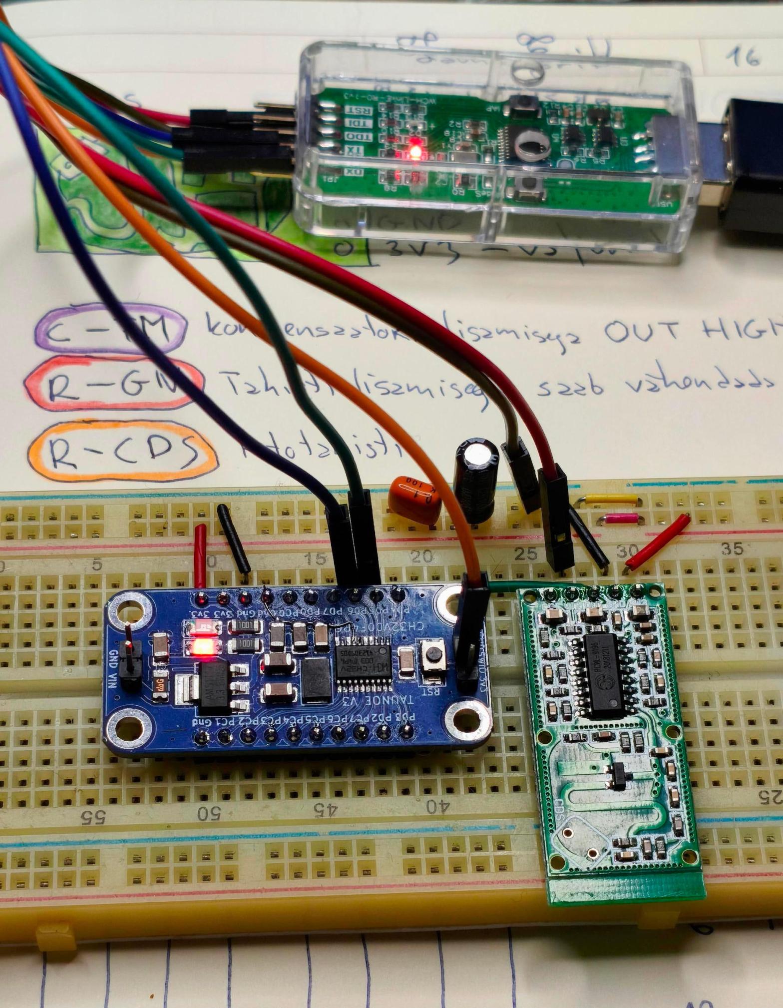
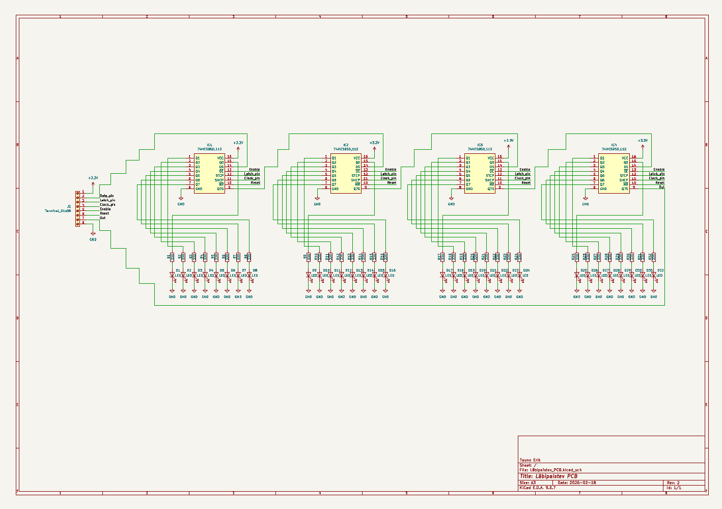
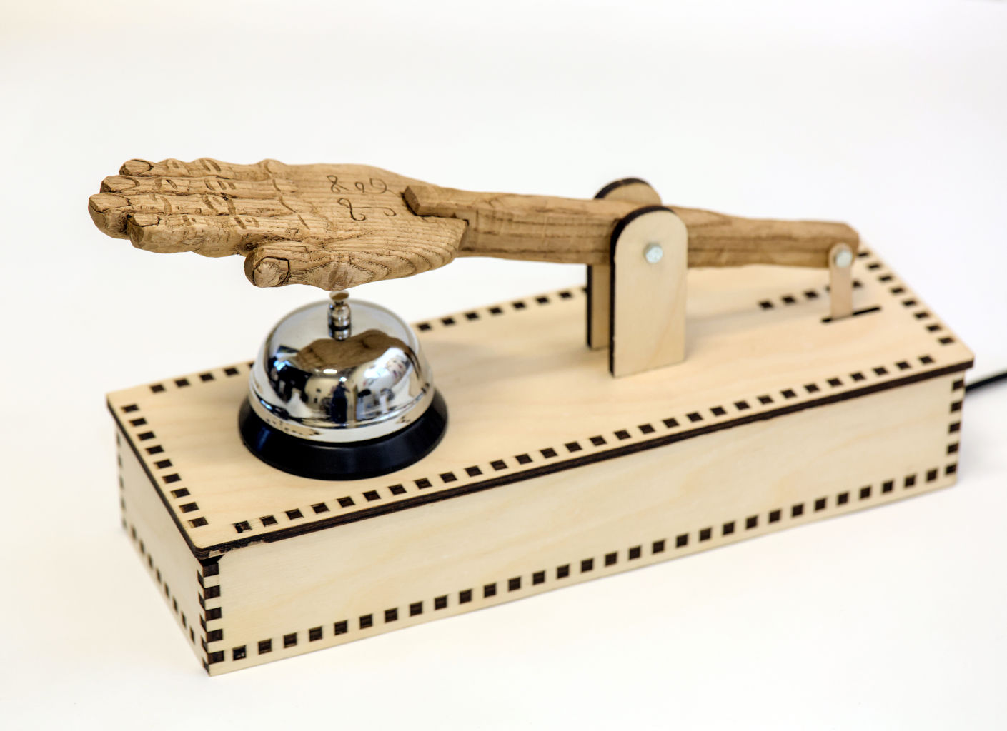
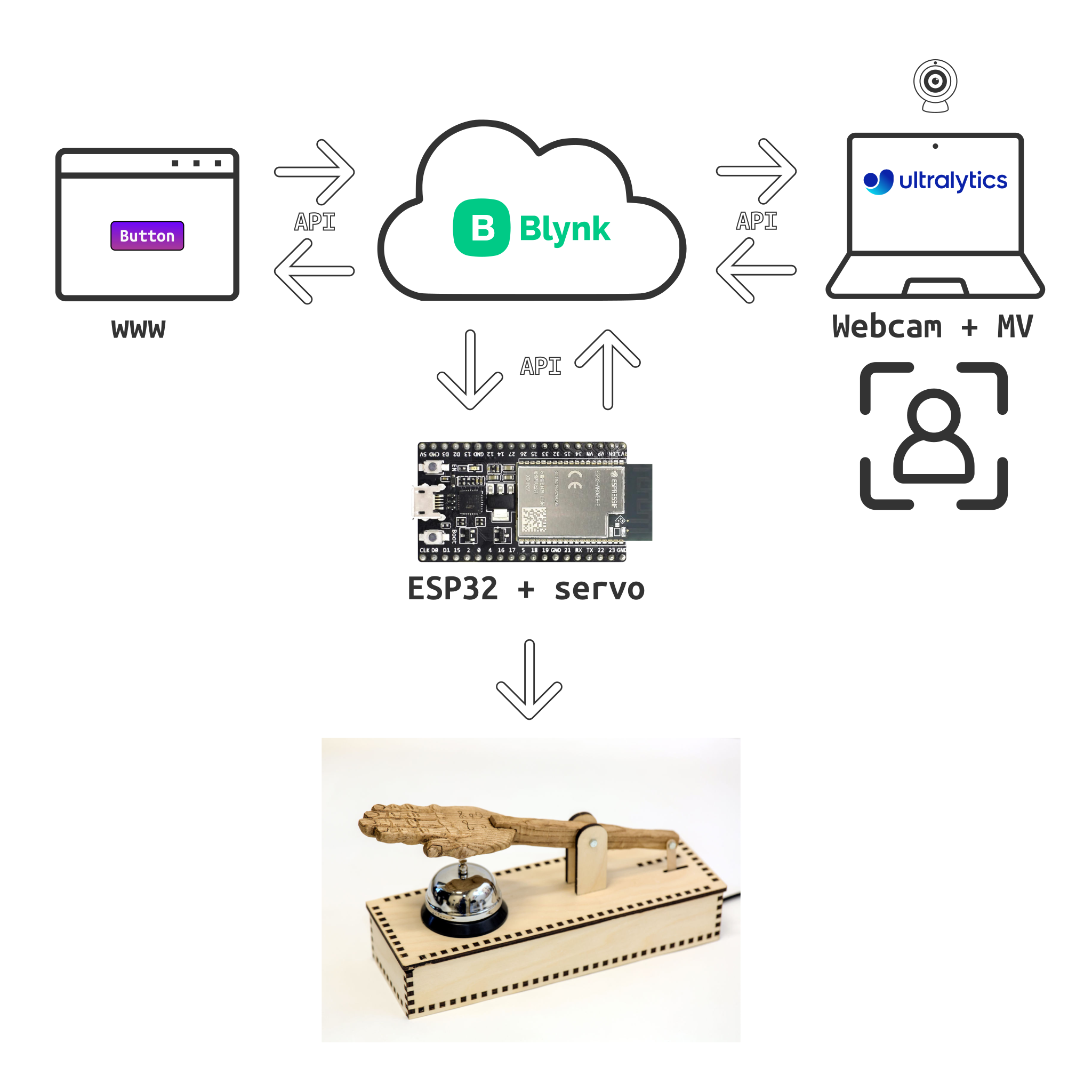
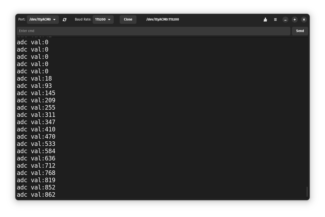
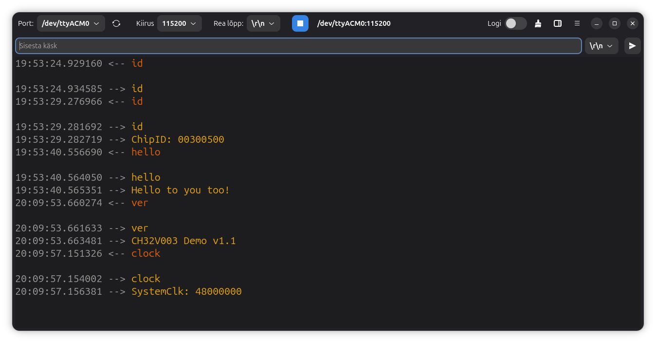
UV weathering chamber

The goal was to build a chamber to test the durability of wooden parts under UV radiation.

The cabinet contains six UV radiation lamps. The upper part contains all the electronics, control elements and fans.

There is one ballast for every two UV lamps. UV lamps operate on 230V alternating current (AC). The second 5V power supply is for the controller. It has a solid-state relay that turns the UV lights on/off using a microcontroller. I use Raspberry Pi Pico 2 W. The plan is to add a web interface in the future. It has a DHT22 temperature and humidity sensor. It is inside the UV chamber. Also, it has a control circuit for the fans (5V). I also added door sensors to automatically turn off the UV light when someone opens the doors.

Initial idea of ​​cabinet design
CAD drawings
CAD drawings

First finished prototype. Made by TSENTER. The material is MDF, painted white. The front panel (and other details) are printed in green.

TSENTR UV weathering chamber

Control panel.

Front panel
Front panel

Wiring and electronics of the first prototype.

Electronics in the upper part
Project schematics
Project schematics

UV lamps in the cabinet.

UV lamps in the cabinet.
UV lamps in the cabinet

For the prototype, I used a PCB that was left over from a previous project. At the same time, I started to design a new PCB for this project. I contain most of the external components that I need for this board. Like a fans control circuit, LED drivers and buttons pull up resistors. All outputs are screw terminals. It is a plain green colour that matches the overall design of the cabinet. The PCB is made and assembled by PCBWay. As always, good quality. It is a simple two-layer board, but it makes it easier to connect different parts.

New PCB for the next prototype.
New board schematics
Designing a new board in KiCad

Transparent PCB

This was made by PCBWay. I designed it in KiCad. It’s basically four shift registers and LEDs. Since it was my first time seeing a transparent PCB, I designed it to explore how it could be used. It’s not transparent like glass. It’s more like translucent and diffuses light. One advantage is that you can see all the tracks.

Mine is without a solder mask. But you can select a transparent solder mask, which is under Advanced PCB.

Pässu and I first look into it:

Test code

This is a test code that uses the CH32V003 microcontroller and MounRiver Studio 2. It shifts round a 1-bit in a 32-bit register to light up the corresponding LED.

#include "debug.h"

// Define our pins on Port C
#define DATA_PIN  GPIO_Pin_0
#define CLOCK_PIN GPIO_Pin_1
#define LATCH_PIN GPIO_Pin_2
#define GPIO_PORT GPIOC


/* Global Variable */
vu8 val;

// Global tick counter
volatile uint32_t global_ms = 0;

/*********************************************************************
 * @fn      USARTx_CFG
 *
 * @brief   Initializes the USART2 & USART3 peripheral.
 *
 * @return  none
 */
void USARTx_CFG(void)
{
    GPIO_InitTypeDef  GPIO_InitStructure = {0};
    USART_InitTypeDef USART_InitStructure = {0};

    RCC_APB2PeriphClockCmd(RCC_APB2Periph_GPIOD | RCC_APB2Periph_USART1, ENABLE);

    /* USART1 TX-->D.5   RX-->D.6 */
    GPIO_InitStructure.GPIO_Pin = GPIO_Pin_5;
    GPIO_InitStructure.GPIO_Speed = GPIO_Speed_30MHz;
    GPIO_InitStructure.GPIO_Mode = GPIO_Mode_AF_PP;
    GPIO_Init(GPIOD, &GPIO_InitStructure);
    GPIO_InitStructure.GPIO_Pin = GPIO_Pin_6;
    GPIO_InitStructure.GPIO_Mode = GPIO_Mode_IN_FLOATING;
    GPIO_Init(GPIOD, &GPIO_InitStructure);

    USART_InitStructure.USART_BaudRate = 115200;
    USART_InitStructure.USART_WordLength = USART_WordLength_8b;
    USART_InitStructure.USART_StopBits = USART_StopBits_1;
    USART_InitStructure.USART_Parity = USART_Parity_No;
    USART_InitStructure.USART_HardwareFlowControl = USART_HardwareFlowControl_None;
    USART_InitStructure.USART_Mode = USART_Mode_Tx | USART_Mode_Rx;

    USART_Init(USART1, &USART_InitStructure);
    USART_Cmd(USART1, ENABLE);
}

// Update the global tick every 1ms
void SysTick_Handler(void) __attribute__((interrupt("WCH-Interrupt-fast")));
void SysTick_Handler(void) {
    global_ms++;
    SysTick->SR = 0; // Clear interrupt flag
}

void SysTick_Init(void) {
    // SystemCoreClock is usually 48MHz
    // Set reload to trigger every 1ms
    SysTick->CMP = SystemCoreClock / 1000;
    SysTick->CNT = 0;
    SysTick->CTLR = 0x0F; // Enable interrupt, enable counter, HCLK as clock
    NVIC_EnableIRQ(SysTick_IRQn);
}

void SPI_1_config(void) {
    GPIO_InitTypeDef GPIO_InitStructure = {0};
    SPI_InitTypeDef  SPI_InitStructure = {0};

    RCC_APB2PeriphClockCmd(RCC_APB2Periph_GPIOC | RCC_APB2Periph_SPI1, ENABLE);

    // PC5 (SCK) & PC6 (MOSI) as Alternate Function Push-Pull
    GPIO_InitStructure.GPIO_Pin = GPIO_Pin_5 | GPIO_Pin_6;
    GPIO_InitStructure.GPIO_Mode = GPIO_Mode_AF_PP;
    GPIO_InitStructure.GPIO_Speed = GPIO_Speed_50MHz;
    GPIO_Init(GPIOC, &GPIO_InitStructure);

    // PC1 (Latch) as standard Output
    GPIO_InitStructure.GPIO_Pin = GPIO_Pin_1;
    GPIO_InitStructure.GPIO_Mode = GPIO_Mode_Out_PP;
    GPIO_Init(GPIOC, &GPIO_InitStructure);

    SPI_InitStructure.SPI_Direction = SPI_Direction_1Line_Tx;
    SPI_InitStructure.SPI_Mode = SPI_Mode_Master;
    SPI_InitStructure.SPI_DataSize = SPI_DataSize_8b;
    SPI_InitStructure.SPI_CPOL = SPI_CPOL_Low;
    SPI_InitStructure.SPI_CPHA = SPI_CPHA_1Edge;
    SPI_InitStructure.SPI_NSS = SPI_NSS_Soft;
    SPI_InitStructure.SPI_BaudRatePrescaler = SPI_BaudRatePrescaler_8; // 3MHz
    SPI_InitStructure.SPI_FirstBit = SPI_FirstBit_MSB;
    SPI_Init(SPI1, &SPI_InitStructure);

    SPI_Cmd(SPI1, ENABLE);
}

void SPI_send_data(uint32_t data) {
    GPIO_WriteBit(GPIOC, GPIO_Pin_1, Bit_RESET); // Latch LOW

    // Send 4 bytes (32 bits)
    for(int i = 3; i >= 0; i--) {
        while(SPI_I2S_GetFlagStatus(SPI1, SPI_I2S_FLAG_TXE) == RESET);
        SPI_I2S_SendData(SPI1, (uint8_t)(data >> (i * 8)));
    }

    // Wait for last byte to finish
    while(SPI_I2S_GetFlagStatus(SPI1, SPI_I2S_FLAG_BSY) == SET);
    GPIO_WriteBit(GPIOC, GPIO_Pin_1, Bit_SET); // Latch HIGH
}

/*********************************************************************
 * @fn      main
 *
 * @brief   Main program.
 *
 * @return  none
 */
int main(void)
{
    NVIC_PriorityGroupConfig(NVIC_PriorityGroup_1); // 2?
    SystemCoreClockUpdate();
    Delay_Init();
 
    SPI_1_config();
    SysTick_Init();

#if (SDI_PRINT == SDI_PR_OPEN)
    SDI_Printf_Enable();
#else
    USART_Printf_Init(115200);
#endif
    printf("SystemClk:%d\r\n",SystemCoreClock);
    printf( "ChipID:%08x\r\n", DBGMCU_GetCHIPID() );

    USARTx_CFG();

  
    uint32_t data = 0x01;
    uint32_t last_update_time = 0;
    const uint32_t interval = 15; // 100ms update rate

    while(1)
    {
        if (global_ms - last_update_time >= interval) {
            last_update_time = global_ms;

            SPI_send_data(data);

            // Rotate bits for a "running light" effect
            data = (data << 1);
            if (data == 0) {
                data = 0x01;
            }
        }
    } // while end
}

Links

DS1307 Real-Time Clock notes

RTC – Real-Time Clock. Counts Seconds, Minutes, Hours, Date of the Month, Month, Day of the Week, and Year with Leap-Year. Compensation Valid Up to 2100.

24-hour or 12-hour format

The contents of the time and calendar registers are in the BCD format. BCD – binary-coded decimal

I2C serial interface. Slave device. Operates in the standard mode (100kHz) only.

Address (7-bit) 1101000 = 0x68 followed by the direction bit (R/W).

Write address (8-bit) 11010000 = 0xD0

Read address (8-bit) 11010001 = 0xD1

Has a built-in power-sense circuit that detects power failures and automatically switches to the backup supply.

56-Byte, Battery-Backed, General-Purpose SRAM with Unlimited Writes

Programmable Square-Wave Output Signal

Consumes Less than 500nA in Battery-Backup Mode with Oscillator Running

RTC and RAM address map

RTC registers 0x00 to 0x07

SRAM registers 0x08 to 0x3F

BIT 7: CH – clock halt pit. When set to 1, the oscillator is disabled.

01/01/00 01 00:00:00 (MM/DD/YY DOW HH:MM:SS)

BIT 6: 1 – 12-hour mode, 0 – 24-hour mode

Testing It with CH32V003

Project code: https://github.com/taunoe/RTC_aeg

Prototüüp

Pi Pico 2 Sensor Project

Project started November 13, 2025.

I gradually added material as the project progressed.

Goal

I need a sensor that can detect whether an object is in the desired location or not. Must use 24V input voltage, common in industry. Pass the signal on to either another microcontroller or a robot. The user must be able to easily adjust the sensitivity or distance of the sensor.

Plan

The plan is to make a custom printed circuit board (PCB) that will hold:

  1. Power module – To convert 24V to a low voltage suitable for the microcontroller. OKY3504-1 Mini-360 DC-DC buck converter 4.75V-23V to 1V-17V step down power module.
  2. Development board – Raspberry Pi Pico 2 RP2350. The board brain.
  3. Sensor – ToF VL53L0X Time Of Flight distance sensor.
  4. Display – To display current sensor readings and user-set parameters. 0.96″, 128×64 px, I2C, OLED Display Module. Driver IC: SSD1306.
  5. Rotary encoders – User input. 360-degree rotation. With a push button.
  6. Indicator LEDs (Red and green) – To quickly interpret sensor readings.
  7. Optocouplers – PC817. Galvanically isolated signal output.
  8. Screw terminals – To connect the sensor, power input, sensor output and other possible connections.

Since this project is still in its early stages, I reserve the right to make changes at a later stage. Therefore, I will add most MCU pins to the PCB.

The first prototype on the breadboard

It uses a Pico 1 (RP2040) clone.

Prototype on a breadboard

Prototype schematics

I designed the schematics and a 2-layer PCB in KiCAD. Added new symbols and footprints to modules that I needed, but didn’t exist in the library. I left the same pin order to symbols as on a real modules. To avoid pin order mistakes. Like on the OLED module, the VCC and GND pins can be in reverse order.

In OnShape, I designed simple 3D models that I exported as STEP files.

Prototype schematics
PCB Schematics
PCB drawing in KiCad
Rotary Encoder 3D model made in OnShape

PCBs

Fortunately, when I designed the prototype, PCBWay contacted me to support PCB fabrication. I have ordered a lot of printed circuit boards from them. And they will always be produced quickly, and the quality is good. I have never had any problems.

KiCAD has a plugin that allows you to quickly upload files to PCBway and place an order. You can directly install it from the KiCad Plugins window. Search “PCBWay”. It makes the ordering process simple. You don’t have to worry about whether you added all the layers and files. I ordered 10 yellow PCBs with a black silk screen. The yellow silk screen is not as bright as I like. But not bad. I like the board colour where there is no copper layer. Maybe next time I order one without copperfill.

My design is now more like a Raspberry Pi Pico expansion board. And maybe next time I will make it smaller and with fewer pins. But now I added them all so I can use it more than one purpose.

PCB front side
PCB back side

Power module

Because the Raspberry Pi Pico input voltage is 1.8V to 5.5V, I needed to configure the power module to the right output voltage. I use the OKY3504-1 DC-to-DC step-down converter. The input voltage is 24V, and the output is 5V.

I set up a breadboard to configure it. There is a little screw on the board for that.

Configuring the power module

Sensor module

I soldered the sensor on a separate PCB. With has screw terminals to connect the cable.
Sensor on protoboard

Case for Sensor v1

I made a simple case for the sensor from plywood. It is made of 4 mm plywood and laser cut.

First case version for the sensor. Back side opened.
First case version for the sensor. Front side.

Assembled PCB

Most components are soldered to the printed circuit board.
Full view of PCB
All essential components are soldered to the PCB.

Project box v1

The first project box consisted of two parts. Connected with the hinge. It was a complicated design and assembly.

Project box at opened state.
Project box at closed state. On the right is the sensor cable.
Project box with a screen and rotary encoders.

Project box v2

In the second version, I simplified the box design. There is now only one box with an acrylic cover.

Project box version 2. The cover is made from acrylic glass. (Text on screen is upside down).

First demo with a new project box:

The working principle of the sensor. The left cnob is to set the min. distance and right one set the max. distance. When the object is between min and max, then the output signal is in the ON state, and the red LED is on.

The working principle of the sensor.

Code

The project code can be found on GitHub: https://github.com/taunoe/pi-pico-andur/tree/main/firmware/PlatfoemIO-Pico-2/Andur

I use PlatformIO and maxgerhardt core. It’s a work in progress now.

Future improvements

  • Add isolated input from the robot or other device.

BELL Project

Bell, Tauno Erik

This is a fun project in which I created a mechanised system to ring a table bell powered by an ESP32 microcontroller and connected to the Blynk IoT cloud platform. The bell can be triggered through the Blynk API.

There are two ways to activate the bell:

Manual Control: I built a simple webpage hosted on GitHub Pages with a button to manually ring the bell.

    Automated System: Using an old laptop with a webcam, I developed an automated system powered by a Python script utilizing the Ultralytics machine vision library. The system detects objects like people, cups, or other items, and when a match is found, it sends a signal to activate the bell.

    Bell, Tauno Erik

    CH32V003 GPIO/Pin modes

    Output modes

    There are two different output modes:

    • Open drain output: GPIO_Mode_Out_OD
    • Push-pull output: GPIO_Mode_Out_PP
    GPIO_InitStructure.GPIO_Mode = GPIO_Mode_Out_PP;

    Input modes

    There are four different input modes:

    • Floating input: GPIO_Mode_IN_FLOATING
    • Pull-up input: GPIO_Mode_IPU
    • Pull-down input: GPIO_Mode_IPD
    • Analog input: GPIO_Mode_AIN
    GPIO_InitStructure.GPIO_Mode = GPIO_Mode_IPU;

    Alternate functions

    The GPIO can also be configured as an “alternate function”. Used for specific hardware functions like pulse width modulation (PWM) or serial peripheral interface (SPI).

    The modes for alternate functions can be:

    • Open drain: GPIO_Mode_AF_OD
    • Push-pull (PWM): GPIO_Mode_AF_PP
    GPIO_InitStructure.GPIO_Mode = GPIO_Mode_AF_PP;

    Speed

    There are three-speed options:

    • GPIO_Speed_2MHz
    • GPIO_Speed_10MHz
    • GPIO_Speed_50MHz
    GPIO_InitStructure.GPIO_Speed = GPIO_Speed_50MHz;

    Output Function

    • GPIO_SetBits – used for setting the GPIO High (1)
    • GPIO_ResetBits – used for setting the GPIO Low (0)
    • GPIO_WriteBit – used when you want to SET (High) and REST (Low) the GPIO with the same function
    • GPIO_Write – to set the complete GPIO port
    • GPIO_PinLockConfig – special function. Helps you lock the pin so that accidentally in other parts of the configuration can’t be changed.
    GPIO_SetBits(GPIOD, GPIO_Pin_0);
    GPIO_ResetBits(GPIOD, GPIO_Pin_0);
    GPIO_WriteBit(GPIOD, GPIO_Pin_0, SET);
    GPIO_WriteBit(GPIOD, GPIO_Pin_0, RESET);
    GPIO_WriteBit(GPIOC, GPIO_Pin_0, 1);

    Input functions

    • GPIO_ReadInputDataBit – used to get the status of a single pin (high or low)
    • GPIO_ReadInputData – used to read the full port
    u8 pin_status = GPIO_ReadInputDataBit(GPIOD, GPIO_Pin_3);

    5V tolerant Pins

    5V tolerant pins are PC1, PC2, PC4, PC5 and PC6.

    PD7 – Reset Pin

    PD7 is by default configured as a reset pin. To change it to a regular GPIO pin:

    FLASH_Unlock();
    FLASH_EraseOptionBytes();
    FLASH_UserOptionByteConfig(OB_STOP_NoRST, OB_STDBY_NoRST, OB_RST_NoEN, OB_PowerON_Start_Mode_USER);
    FLASH_Unlock();
    Hardware setup. Tauno Erik

    Code

    /********************************** (C) COPYRIGHT *******************************
     * File Name          : main.c
     * Date               : 15.07.2024
     * Autor              : Tauno Erik
     * Description        : GPIO Input/Output
    *********************************************************************************/
    
    #include "debug.h"
    
    /* Global define */
    #define HIGH   1
    #define LOW    0
    
    #define INPUT  0
    #define OUTPUT 1
    
    #define PC0    0
    #define PC1    1
    #define PC2    2
    #define PC3    3
    #define PC4    4
    #define PC5    5
    #define PC6    6
    #define PC7    7
    #define PD0    8
    #define PD1    9
    #define PD2   10
    #define PD3   11
    #define PD4   12
    #define PD5   13
    #define PD6   14
    #define PD7   15  // RST
    #define PA1   16  // X1
    #define PA2   17  // X0
    
    /*********************************************************************
     * @fn      get_chip_type
     *
     * @brief   Returns the CHIP identifier.
     *
     * @return Device identifier.
     *    ChipID List-
     *      CH32V003F4P6-0x003005x0
     *      CH32V003F4U6-0x003105x0
     *      CH32V003A4M6-0x003205x0
     *      J4M6-0x003305x0
     */
    uint32_t get_chip_type( void )
    {
      return( *( uint32_t * )0x1FFFF7C4 );
    }
    
    uint16_t get_MCU_flash_size( void )
    {
      return( *( uint16_t * )0x1FFFF7E0 );
    }
    
    uint32_t get_MCU_uid_1( void )
    {
      return( *( uint32_t * )0x1FFFF7E8 );
    }
    
    uint32_t get_MCU_uid_2( void )
    {
      return( *( uint32_t * )0x1FFFF7EC );
    }
    
    uint32_t get_MCU_uid_3( void )
    {
        return( *( uint32_t * )0x1FFFF7F0 );
    }
    
    /*****************************************************************************************
    */
    u8 tauno_PIN_read(u8 pin)
    {
      u8 val = LOW;
      
      switch (pin)
      {
        case PA1:  // X0
          val = GPIO_ReadInputDataBit(GPIOA, GPIO_Pin_1);
          break;
        case PA2:  // X1
          val = GPIO_ReadInputDataBit(GPIOA, GPIO_Pin_2);
          break;
        case PC0:
          val = GPIO_ReadInputDataBit(GPIOC, GPIO_Pin_0);
          break;
        case PC1:
          val = GPIO_ReadInputDataBit(GPIOC, GPIO_Pin_1);
          break;
        case PC2:
          val = GPIO_ReadInputDataBit(GPIOC, GPIO_Pin_2);
          break;
        case PC3:
          val = GPIO_ReadInputDataBit(GPIOC, GPIO_Pin_3);
          break;
        case PC4:
          val = GPIO_ReadInputDataBit(GPIOC, GPIO_Pin_4);
          break;
        case PC5:
          val = GPIO_ReadInputDataBit(GPIOC, GPIO_Pin_5);
          break;
        case PC6:
          val = GPIO_ReadInputDataBit(GPIOC, GPIO_Pin_6);
          break;
        case PC7:
          val = GPIO_ReadInputDataBit(GPIOC, GPIO_Pin_7);
          break;
        case PD0:
          val = GPIO_ReadInputDataBit(GPIOD, GPIO_Pin_0);
          break;
        case PD1:
          val = GPIO_ReadInputDataBit(GPIOD, GPIO_Pin_1);
          break;
        case PD2:
          val = GPIO_ReadInputDataBit(GPIOD, GPIO_Pin_2);
          break;
        case PD3:
          val = GPIO_ReadInputDataBit(GPIOD, GPIO_Pin_3);
          break;
        case PD4:
          val = GPIO_ReadInputDataBit(GPIOD, GPIO_Pin_4);
          break;
        case PD5:
          val = GPIO_ReadInputDataBit(GPIOD, GPIO_Pin_5);
          break;
        case PD6:
          val = GPIO_ReadInputDataBit(GPIOD, GPIO_Pin_6);
          break;
        case PD7:  // RST
          val = GPIO_ReadInputDataBit(GPIOD, GPIO_Pin_7);
          break;
        default:
          break;
      }
      
      return val;
    }
    
    /*****************************************************************************************
    */
    void tauno_PIN_write(u8 pin, u8 value)
    {
      switch (pin)
      {
        case PC0:
          GPIO_WriteBit(GPIOC, GPIO_Pin_0, value);
          break;
        case PC1:
          GPIO_WriteBit(GPIOC, GPIO_Pin_1, value);
          break;
        case PC2:
          GPIO_WriteBit(GPIOC, GPIO_Pin_2, value);
          break;
        case PC3:
          GPIO_WriteBit(GPIOC, GPIO_Pin_3, value);
          break;
        case PC4:
          GPIO_WriteBit(GPIOC, GPIO_Pin_4, value);
          break;
        case PC5:
          GPIO_WriteBit(GPIOC, GPIO_Pin_5, value);
          break;
        case PC6:
          GPIO_WriteBit(GPIOC, GPIO_Pin_6, value);
          break;
        case PC7:
          GPIO_WriteBit(GPIOC, GPIO_Pin_7, value);
          break;
        case PD0:
          GPIO_WriteBit(GPIOD, GPIO_Pin_0, value);
          break;
        case PD1:
          GPIO_WriteBit(GPIOD, GPIO_Pin_1, value);
          break;
        case PD2:
          GPIO_WriteBit(GPIOD, GPIO_Pin_2, value);
          break;
        case PD3:
          GPIO_WriteBit(GPIOD, GPIO_Pin_3, value);
          break;
        case PD4:
          GPIO_WriteBit(GPIOD, GPIO_Pin_4, value);
          break;
        case PD5:
          GPIO_WriteBit(GPIOD, GPIO_Pin_5, value);
          break;
        case PD6:
          GPIO_WriteBit(GPIOD, GPIO_Pin_6, value);
          break;
        case PD7:  // RST pin
          GPIO_WriteBit(GPIOD, GPIO_Pin_7, value);
          break;
        case PA1:  // External crystal
          GPIO_WriteBit(GPIOA, GPIO_Pin_1, value);
          break;
        case PA2:  // External crystal
          GPIO_WriteBit(GPIOA, GPIO_Pin_2, value);
          break;
        default:
          break;
      }
    }
    
    /*****************************************************************************************
    */
    void tauno_pin_init(u8 pin, u8 mode)
    {
      GPIO_InitTypeDef GPIO_InitStructure = {0}; // Variable used for the GPIO configuration
      
      switch (pin)
      {
        case PA1:  // X0
          RCC_APB2PeriphClockCmd(RCC_APB2Periph_GPIOA, ENABLE);  // Enable the clock for Port
          GPIO_InitStructure.GPIO_Pin = GPIO_Pin_1; // pin
          break;
        case PA2:  // X1
          RCC_APB2PeriphClockCmd(RCC_APB2Periph_GPIOA, ENABLE);  // Enable the clock for Port
          GPIO_InitStructure.GPIO_Pin = GPIO_Pin_2; // pin
          break;
        case PC0:
          RCC_APB2PeriphClockCmd(RCC_APB2Periph_GPIOC, ENABLE);  // Enable the clock for Port
          GPIO_InitStructure.GPIO_Pin = GPIO_Pin_0; // pin
          break;
        case PC1:
          RCC_APB2PeriphClockCmd(RCC_APB2Periph_GPIOC, ENABLE);  // Enable the clock for Port
          GPIO_InitStructure.GPIO_Pin = GPIO_Pin_1; // pin
          break;
        case PC2:
          RCC_APB2PeriphClockCmd(RCC_APB2Periph_GPIOC, ENABLE);  // Enable the clock for Port
          GPIO_InitStructure.GPIO_Pin = GPIO_Pin_2; // pin
          break;
        case PC3:
          RCC_APB2PeriphClockCmd(RCC_APB2Periph_GPIOC, ENABLE);  // Enable the clock for Port
          GPIO_InitStructure.GPIO_Pin = GPIO_Pin_3; // pin
          break;
        case PC4:
          RCC_APB2PeriphClockCmd(RCC_APB2Periph_GPIOC, ENABLE);  // Enable the clock for Port
          GPIO_InitStructure.GPIO_Pin = GPIO_Pin_4; // pin
          break;
        case PC5:
          RCC_APB2PeriphClockCmd(RCC_APB2Periph_GPIOC, ENABLE);  // Enable the clock for Port
          GPIO_InitStructure.GPIO_Pin = GPIO_Pin_5; // pin
          break;
        case PC6:
          RCC_APB2PeriphClockCmd(RCC_APB2Periph_GPIOC, ENABLE);  // Enable the clock for Port
          GPIO_InitStructure.GPIO_Pin = GPIO_Pin_6; // pin
          break;
        case PC7:
          RCC_APB2PeriphClockCmd(RCC_APB2Periph_GPIOC, ENABLE);  // Enable the clock for Port
          GPIO_InitStructure.GPIO_Pin = GPIO_Pin_7; // pin
          break;
        case PD0:
          RCC_APB2PeriphClockCmd(RCC_APB2Periph_GPIOD, ENABLE);  // Enable the clock for Port
          GPIO_InitStructure.GPIO_Pin = GPIO_Pin_0; // pin
          break;
        case PD1:
          RCC_APB2PeriphClockCmd(RCC_APB2Periph_GPIOD, ENABLE);  // Enable the clock for Port
          GPIO_InitStructure.GPIO_Pin = GPIO_Pin_1; // pin
          break;
        case PD2:
          RCC_APB2PeriphClockCmd(RCC_APB2Periph_GPIOD, ENABLE);  // Enable the clock for Port
          GPIO_InitStructure.GPIO_Pin = GPIO_Pin_2; // pin
          break;
        case PD3:
          RCC_APB2PeriphClockCmd(RCC_APB2Periph_GPIOD, ENABLE);  // Enable the clock for Port
          GPIO_InitStructure.GPIO_Pin = GPIO_Pin_3; // pin
          break;
        case PD4:
          RCC_APB2PeriphClockCmd(RCC_APB2Periph_GPIOD, ENABLE);  // Enable the clock for Port
          GPIO_InitStructure.GPIO_Pin = GPIO_Pin_4; // pin
          break;
        case PD5:
          RCC_APB2PeriphClockCmd(RCC_APB2Periph_GPIOD, ENABLE);  // Enable the clock for Port
          GPIO_InitStructure.GPIO_Pin = GPIO_Pin_5; // pin
          break;
        case PD6:
          RCC_APB2PeriphClockCmd(RCC_APB2Periph_GPIOD, ENABLE);  // Enable the clock for Port
          GPIO_InitStructure.GPIO_Pin = GPIO_Pin_6; // pin
          break;
        case PD7:  // RST
          RCC_APB2PeriphClockCmd(RCC_APB2Periph_GPIOD, ENABLE);  // Enable the clock for Port
          GPIO_InitStructure.GPIO_Pin = GPIO_Pin_7; // pin
          break;
        default:
          break;
      }
      
      if (mode == OUTPUT)
      {
        GPIO_InitStructure.GPIO_Mode = GPIO_Mode_Out_PP;  // Push-pull output
      } 
      else
      {
        GPIO_InitStructure.GPIO_Mode = GPIO_Mode_IPU;  // Pull-up input
      }
    
      // Speed
      GPIO_InitStructure.GPIO_Speed = GPIO_Speed_50MHz;
    
      switch (pin)
      {
        case PA1:  // X0
        case PA2:  // X1
          GPIO_Init(GPIOA, &GPIO_InitStructure);
          break;
        case PC0:
        case PC1:
        case PC2:
        case PC3:
        case PC4:
        case PC5:
        case PC6:
        case PC7:
          GPIO_Init(GPIOC, &GPIO_InitStructure);
          break;
        case PD0:
        case PD1:
        case PD2:
        case PD3:
        case PD4:
        case PD5:
        case PD6:
        case PD7:  // RST
          GPIO_Init(GPIOD, &GPIO_InitStructure);
          break;
        default:
          break;
      }
    }
    
    /*****************************************************************************************
    */
    int main(void) {
      u8 write_status = LOW;
      u8 read_status = LOW;
    
      NVIC_PriorityGroupConfig(NVIC_PriorityGroup_2);
      Delay_Init();
      USART_Printf_Init(115200);
      Delay_Ms(3000);  // Give serial monitor time to open
    
      printf("Flash size: \t%d\r\n", (unsigned)get_MCU_flash_size);
      printf("SystemClk: \t%d\r\n", (unsigned)SystemCoreClock);
      printf("Device ID: \t%08x\r\n", (unsigned)DBGMCU_GetDEVID());
      printf("Revision ID: \t%08x\r\n", (unsigned)DBGMCU_GetREVID());
      printf("Chip type: \t%08x\r\n", (unsigned)get_chip_type());
      printf("UID 1: \t\t%d\r\n", (unsigned)get_MCU_uid_1);
      printf("UID 2: \t\t%d\r\n", (unsigned)get_MCU_uid_2);
      printf("UID 3: \t\t%d\r\n", (unsigned)get_MCU_uid_3);
    
      printf("GPIO Toggle\r\n");
      
      tauno_pin_init(PD0, OUTPUT);
      tauno_pin_init(PC3, INPUT);
    
      while(1)
      {
        Delay_Ms(100);
        read_status = tauno_PIN_read(PC3);
        
        if (read_status == LOW)  // Button bressed
        {
          write_status = HIGH;
          // printf("1\r\n");
          printf("BUTTON\r\n");
        }
        else
        {
          write_status = LOW;
          // printf("0\r\n");
        }
    
        tauno_PIN_write(PD0, write_status);
      }
    }
    
    
    Tauno Erik: Tauno Monitor

    External links

    CH32V003 Analog Reading

    ADC (Analog-to-Digital Converter): Converts an analog signal (such as a voltage) into a digital value that can be processed by a microcontroller. The conversion process typically involves sampling the analog signal at a specific rate and quantizing the signal to produce a digital representation.

    CH32V003 ADC has a 10-bit resolution. Values 0-1023.

    DMA (Direct Memory Access): This is a feature that allows the transfer of data directly to or from memory without involving the CPU. The DMA controller can move data between memory and peripherals autonomously, freeing the CPU to perform other tasks and increasing the efficiency of data transfers.

    When combined, ADC DMA refers to a setup where the ADC performs analog-to-digital conversions, and the resulting digital data is transferred directly to memory using DMA.

    I am using Embeetle IDE for programming and Tauno Monitor for Serial Monitor.

    I use my custom-made CH32V003 development board. However, the code should work on all boards that use this MCU. It has 8 ADC channels (Pins). We can not use ADC channels 0 and 1 if the external crystal is connected, like on my board.

    My test setup:

    This is my main.c file.

    /*********************************************************************
     * File Name          : main.c
     * Board              : ch32v003
     * Date               : 13.07.2024
     * Description        : ADC DMA example
    **********************************************************************/
    
    #include "debug.h"
    
    /* Global Variable */
    u16 TxBuf[10];
    // Pin: PA2 - channel 0 can not be used if the external crystal is connected
    //      PA1 - channel 1 can not be used if the external crystal is connected
    //      PC4 - channel 2
    //      PD2 - channel 3
    //      PD3 - channel 4
    //      PD5 - channel 5
    //      PD6 - channel 6
    //      PD4 - channel 7
    u8 channel = 7;
    
    /*********************************************************************
     * @fn      ADC_Init
     *
     * @brief   Initializes ADC collection.
     *
     * @param   channel - ADC channel.
     *
     * @return  none
     */
    void tauno_ADC_init(u8 channel)
    {
      ADC_InitTypeDef  ADC_InitStructure = {0};
      GPIO_InitTypeDef GPIO_InitStructure = {0};
      
      switch (channel) {
        case 0:  // PA2
        case 1:  // PA1
          RCC_APB2PeriphClockCmd(RCC_APB2Periph_GPIOA, ENABLE);
          break;
        case 2:  // PC4
          RCC_APB2PeriphClockCmd(RCC_APB2Periph_GPIOC, ENABLE);
          break;
        case 3:  // PD2
        case 4:  // PD3
        case 5:  // PD5
        case 6:  // PD6
        case 7:  // PD4
          RCC_APB2PeriphClockCmd(RCC_APB2Periph_GPIOD, ENABLE);
          break;
        default:
          break;
      }
    
      RCC_APB2PeriphClockCmd(RCC_APB2Periph_ADC1, ENABLE);
      RCC_ADCCLKConfig(RCC_PCLK2_Div8);
    
      switch (channel) {
        case 0:  // PA2
          GPIO_InitStructure.GPIO_Pin = GPIO_Pin_2;
          break;
        case 1:  // PA1
          GPIO_InitStructure.GPIO_Pin = GPIO_Pin_1;
          break;
        case 2:  // PC4
          GPIO_InitStructure.GPIO_Pin = GPIO_Pin_4;
          break;
        case 3:  // PD2
          GPIO_InitStructure.GPIO_Pin = GPIO_Pin_2;
          break;
        case 4:  // PD3
          GPIO_InitStructure.GPIO_Pin = GPIO_Pin_3;
          break;
        case 5:  // PD5
          GPIO_InitStructure.GPIO_Pin = GPIO_Pin_5;
          break;
        case 6:  // PD6
          GPIO_InitStructure.GPIO_Pin = GPIO_Pin_6;
          break;
        case 7:  // PD4
          GPIO_InitStructure.GPIO_Pin = GPIO_Pin_4;
          break;
        default:
          break;
      }
      
      GPIO_InitStructure.GPIO_Mode = GPIO_Mode_AIN;
      
      switch (channel) {
        case 0:  // PA2
        case 1:  // PA1
          GPIO_Init(GPIOA, &GPIO_InitStructure);
          break;
        case 2:  // PC4
          GPIO_Init(GPIOC, &GPIO_InitStructure);
          break;
        case 3:  // PD2
        case 4:  // PD3
        case 5:  // PD5
        case 6:  // PD6
        case 7:  // PD4
          GPIO_Init(GPIOD, &GPIO_InitStructure);
          break;
        default:
          break;
      }
    
      ADC_DeInit(ADC1);
      ADC_InitStructure.ADC_Mode = ADC_Mode_Independent;
      ADC_InitStructure.ADC_ScanConvMode = DISABLE;
      ADC_InitStructure.ADC_ContinuousConvMode = ENABLE;
      ADC_InitStructure.ADC_ExternalTrigConv = ADC_ExternalTrigConv_None;
      ADC_InitStructure.ADC_DataAlign = ADC_DataAlign_Right;
      ADC_InitStructure.ADC_NbrOfChannel = 1;
      ADC_Init(ADC1, &ADC_InitStructure);
    
      ADC_Calibration_Vol(ADC1, ADC_CALVOL_50PERCENT);
      ADC_DMACmd(ADC1, ENABLE);
      ADC_Cmd(ADC1, ENABLE);
    
      ADC_ResetCalibration(ADC1);
      while(ADC_GetResetCalibrationStatus(ADC1));
      ADC_StartCalibration(ADC1);
      while(ADC_GetCalibrationStatus(ADC1));
      
      //s16 Calibrattion_Val = Get_CalibrationValue(ADC1); ????
    }
    
    /*********************************************************************
     * @fn      Get_ADC_Val
     *
     * @brief   Returns ADCx conversion result data.
     *
     * @param   ch - ADC channel.
     *            ADC_Channel_0 - ADC Channel0 selected.
     *            ADC_Channel_1 - ADC Channel1 selected.
     *            ADC_Channel_2 - ADC Channel2 selected.
     *            ADC_Channel_3 - ADC Channel3 selected.
     *            ADC_Channel_4 - ADC Channel4 selected.
     *            ADC_Channel_5 - ADC Channel5 selected.
     *            ADC_Channel_6 - ADC Channel6 selected.
     *            ADC_Channel_7 - ADC Channel7 selected.
     *            ADC_Channel_8 - ADC Channel8 selected.
     *            ADC_Channel_9 - ADC Channel9 selected.
     *
     * @return  val
     */
    u16 Get_ADC_Val(u8 channel)
    {
      u16 val;
    
      ADC_RegularChannelConfig(ADC1, channel, 1, ADC_SampleTime_241Cycles);
      ADC_SoftwareStartConvCmd(ADC1, ENABLE);
    
      while(!ADC_GetFlagStatus(ADC1, ADC_FLAG_EOC));
      val = ADC_GetConversionValue(ADC1);
    
      return val;
    }
    
    /*
     * https://github.com/Community-PIO-CH32V/platform-ch32v/blob/develop/examples/adc-cpu-temp-none-os/src/main.c
     */
    u16 Get_ADC_Average(u8 ch, u8 times)
    {
      u32 temp_val = 0;
      u8 t;
      u16 val;
    
      for (t = 0; t < times; t++)
      {
        temp_val += Get_ADC_Val(ch);
        Delay_Ms(5);
      }
    
      val = temp_val / times;
    
      return val;
    }
    
    /*********************************************************************
     * @fn      DMA_Tx_Init
     *
     * @brief   Initializes the DMAy Channelx configuration.
     *
     * @param   DMA_CHx - x can be 1 to 7.
     *          ppadr - Peripheral base address.
     *          memadr - Memory base address.
     *          bufsize - DMA channel buffer size.
     *
     * @return  none
     */
    void DMA_Tx_Init(DMA_Channel_TypeDef *DMA_CHx, u32 ppadr, u32 memadr, u16 bufsize)
    {
        DMA_InitTypeDef DMA_InitStructure = {0};
    
        RCC_AHBPeriphClockCmd(RCC_AHBPeriph_DMA1, ENABLE);
    
        DMA_DeInit(DMA_CHx);
        DMA_InitStructure.DMA_PeripheralBaseAddr = ppadr;
        DMA_InitStructure.DMA_MemoryBaseAddr = memadr;
        DMA_InitStructure.DMA_DIR = DMA_DIR_PeripheralSRC;
        DMA_InitStructure.DMA_BufferSize = bufsize;
        DMA_InitStructure.DMA_PeripheralInc = DMA_PeripheralInc_Disable;
        DMA_InitStructure.DMA_MemoryInc = DMA_MemoryInc_Enable;
        DMA_InitStructure.DMA_PeripheralDataSize = DMA_PeripheralDataSize_HalfWord;
        DMA_InitStructure.DMA_MemoryDataSize = DMA_MemoryDataSize_HalfWord;
        DMA_InitStructure.DMA_Mode = DMA_Mode_Normal;
        DMA_InitStructure.DMA_Priority = DMA_Priority_VeryHigh;
        DMA_InitStructure.DMA_M2M = DMA_M2M_Disable;
        DMA_Init(DMA_CHx, &DMA_InitStructure);
    }
    
    /*********************************************************************
     * @fn      main
     *
     * @brief   Main program.
     *
     * @return  none
     */
    int main(void) {
      u16 adc_val;  // 0-1023
      u16 i;
    
      Delay_Init();
      USART_Printf_Init(115200);
      Delay_Ms(3000);  // Give serial monitor time to open
      printf("SystemClk:%d\r\n", (unsigned)SystemCoreClock);
      printf("DeviceID: %08x\r\n", (unsigned)DBGMCU_GetDEVID());
    
      tauno_ADC_init(channel);
    
      DMA_Tx_Init(DMA1_Channel1, (u32)&ADC1->RDATAR, (u32)TxBuf, 10);
      DMA_Cmd(DMA1_Channel1, ENABLE);
    
      ADC_RegularChannelConfig(ADC1, ADC_Channel_2, 1, ADC_SampleTime_241Cycles);
      ADC_SoftwareStartConvCmd(ADC1, ENABLE);
      Delay_Ms(50);
      ADC_SoftwareStartConvCmd(ADC1, DISABLE);
    
      for (i = 0; i < 10; i++) {
        printf("%04d\r\n", TxBuf[i]);
        Delay_Ms(10);
      }
    
      while (1) {
        adc_val = Get_ADC_Val(channel);
        printf("adc val:%d\r\n", adc_val);
        Delay_Ms(100);
      }
      return 0;
    }
    

    How to install EdSim51DI on Pop OS or Ubuntu

    EdSim51DI is an 8051 microcontroller simulator, developed by James Rogers.

    1. Install java:
    sudo apt update
    sudo apt install default-jdk

    2. Check if OpenJDK JRE was properly installed:

    java -version

    3. Download the EdSim51DI simulator from: http://www.edsim51.com/installationInstructions.html

    4. UnZip file

    5. Give permission to execute the “jar” file as a program.

    6. Open the terminal and navigate to the folder and run:

    java -jar edsim51di.jar

    And it works!

    LED Valgusti WS2811 kiipidega

    Üks LED valgusti 15 LEDiga. LEDe juhitakse läbi WS2811 kiipide, mis lubab kõikide LEDide heledust kontrollida individuaalselt. Tahaküljele saab kinnitada ka Seeedstudi XIAO arendusplaadi. Või siis kontrollida eraldi oleva mikrokontrolleriga. Mina kasutan siin ESP32te. Neid valgusteid saab ka järjestiku mitu tükki üksteise järgi. PCBd valmistas ja printis PCBWay. Komponendid jootsin ise. PCB läbimõõt 10cm.

    ESP-IDF install on Linux

    IDF – IoT Development Framework

    ESP-IDF is Espressif’s official IoT Development Framework for the ESP32, ESP32-S, ESP32-C and ESP32-H series. It provides a self-sufficient SDK for any generic application development on these platforms, using programming languages such as C and C++.

    Install Prerequisites

    sudo apt-get install git wget flex bison gperf python3 python3-pip python3-venv cmake ninja-build ccache libffi-dev libssl-dev dfu-util libusb-1.0-0

    Visual Studio Code

    Install the ESP-IDF Extension.

    In Visual Studio Code, select menu “View” and “Command Palette” and type: configure esp-idf extension

    Choose Express

    Select ESP-IDF version.

    Install.

    For Linux users, OpenOCD needs to add 60-openocd.rules for permission delegation in USB devices to be added in /etc/udev/rules.d/

    sudo cp -n /home/taunoerik/.espressif/tools/openocd-esp32/v0.12.0-esp32-20230921/openocd-esp32/share/openocd/contrib/60-openocd.rules /etc/udev/rules.d

    Basic use

    Create project using example blink” button.

    Create and select folder Blink.

    Select an Espressif target (esp32, esp32s2, etc.) with the ESP-IDF: Set Espressif Device Target command. Default is esp32.

    Configure your project using menuconfig. Use the ESP-IDF: SDK Configuration Editor command (CTRL E G keyboard shortcut ) where the user can modify the ESP-IDF project settings.

    Open the project configuration menu (idf.py menuconfig).

    Build the project, use the ESP-IDF: Build your Project command (CTRL E B keyboard shortcut).

    Blink example code

    #include <stdio.h>
    #include "freertos/FreeRTOS.h"
    #include "freertos/task.h"
    #include "driver/gpio.h"
    #include "esp_log.h"
    #include "led_strip.h"
    #include "sdkconfig.h"
    
    static const char *TAG = "example";
    
    /* Use project configuration menu (idf.py menuconfig) to choose the GPIO to blink,
       or you can edit the following line and set a number here.
    */
    #define BLINK_GPIO 2  // pin
    
    static uint8_t s_led_state = 0;
    
    
    static void blink_led(void) {
        /* Set the GPIO level according to the state (LOW or HIGH)*/
        gpio_set_level(BLINK_GPIO, s_led_state);
    }
    
    static void configure_led(void) {
        ESP_LOGI(TAG, "Blink GPIO LED!");
        gpio_reset_pin(BLINK_GPIO);
        /* Set the GPIO as a push/pull output */
        gpio_set_direction(BLINK_GPIO, GPIO_MODE_OUTPUT);
    }
    
    
    void app_main(void) {
        /* Configure the peripheral according to the LED type */
        configure_led();
    
        while (1) {
          ESP_LOGI(TAG, "Turning the LED %s!", s_led_state == true ? "ON" : "OFF");
          blink_led();
    
          /* Toggle the LED state */
          s_led_state = !s_led_state;
          vTaskDelay(CONFIG_BLINK_PERIOD / portTICK_PERIOD_MS);
        }
    }
    

    Links